4) Introduction to Computer Architectures#
Last time:
Introduction to Linux File System and commands
Today:
1. Architectures#
A von Neumann Architecture:#

The original document by von Neumann in 1945 describes a design architecture for an electronic digital computer with these components:
A processing unit with both an arithmetic logic unit and processor registers
A control unit that includes an instruction register and a program counter
Memory that stores data and instructions
External mass storage
Input and output mechanisms
The term von Neumann architecture has evolved to refer to any stored-program computer in which an instruction fetch and a data operation cannot occur at the same time (since they share a common bus). This is referred to as the von Neumann bottleneck, which often limits the performance of the corresponding system.
A stored-program computer uses the same underlying mechanism to encode both program instructions and data as opposed to designs which use a mechanism such as discrete plugboard wiring or fixed control circuitry for instruction implementation.
The vast majority of modern computers use the same hardware mechanism to encode and store both data and program instructions, but have caches between the CPU and memory, and, for the caches closest to the CPU, have separate caches for instructions and data, so that most instruction and data fetches use separate buses (split-cache architecture).
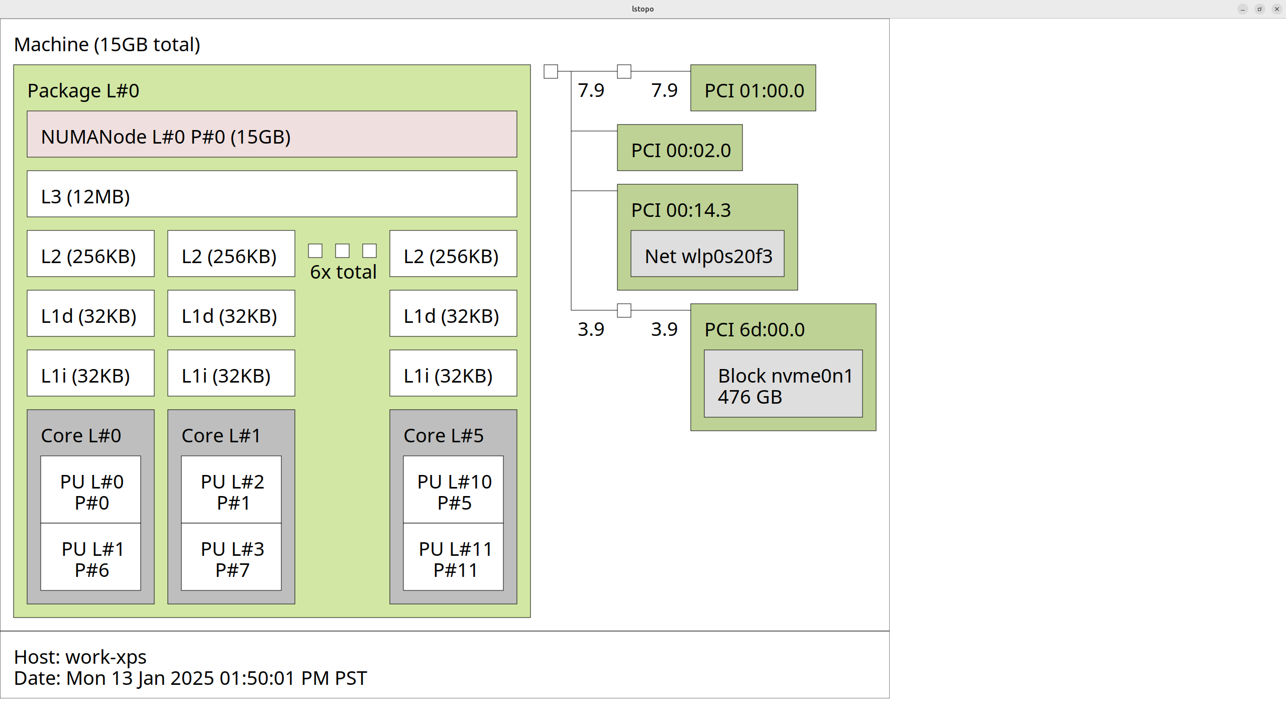
A contemporary architecture:#
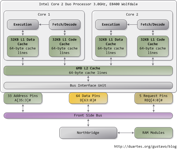
My laptop:#
We can get this kind of information for our machine using hwloc, which provides a library as well as the command-line tool lstopo.
lstopo --output-format svg > lstopo-my_laptop_architecture.svg
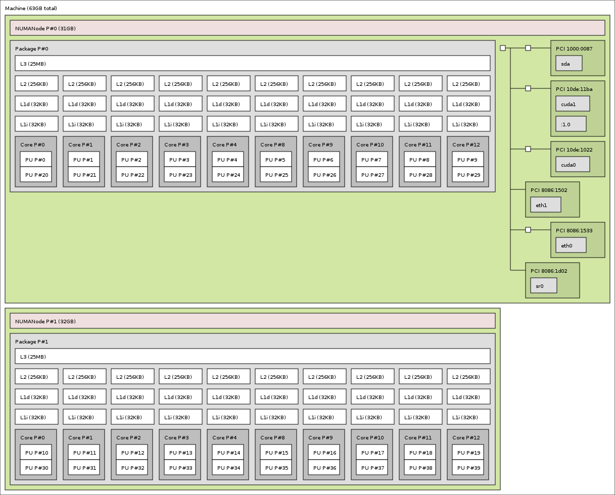
A double-socket compute node with two GPUs:#
2x Xeon Ivy-Bridge-EP E5-2680v2 + 2x NVIDIA GPUs (from 2013, with hwloc v1.11).
GPUs are reported as CUDA devices and X11 display :1.0: (from the hwloc gallery)
Block diagrams:#
A block diagram from a vendor can include additional information about how cores are physically connected.
Ring bus (Xeon E5-2600 family):#
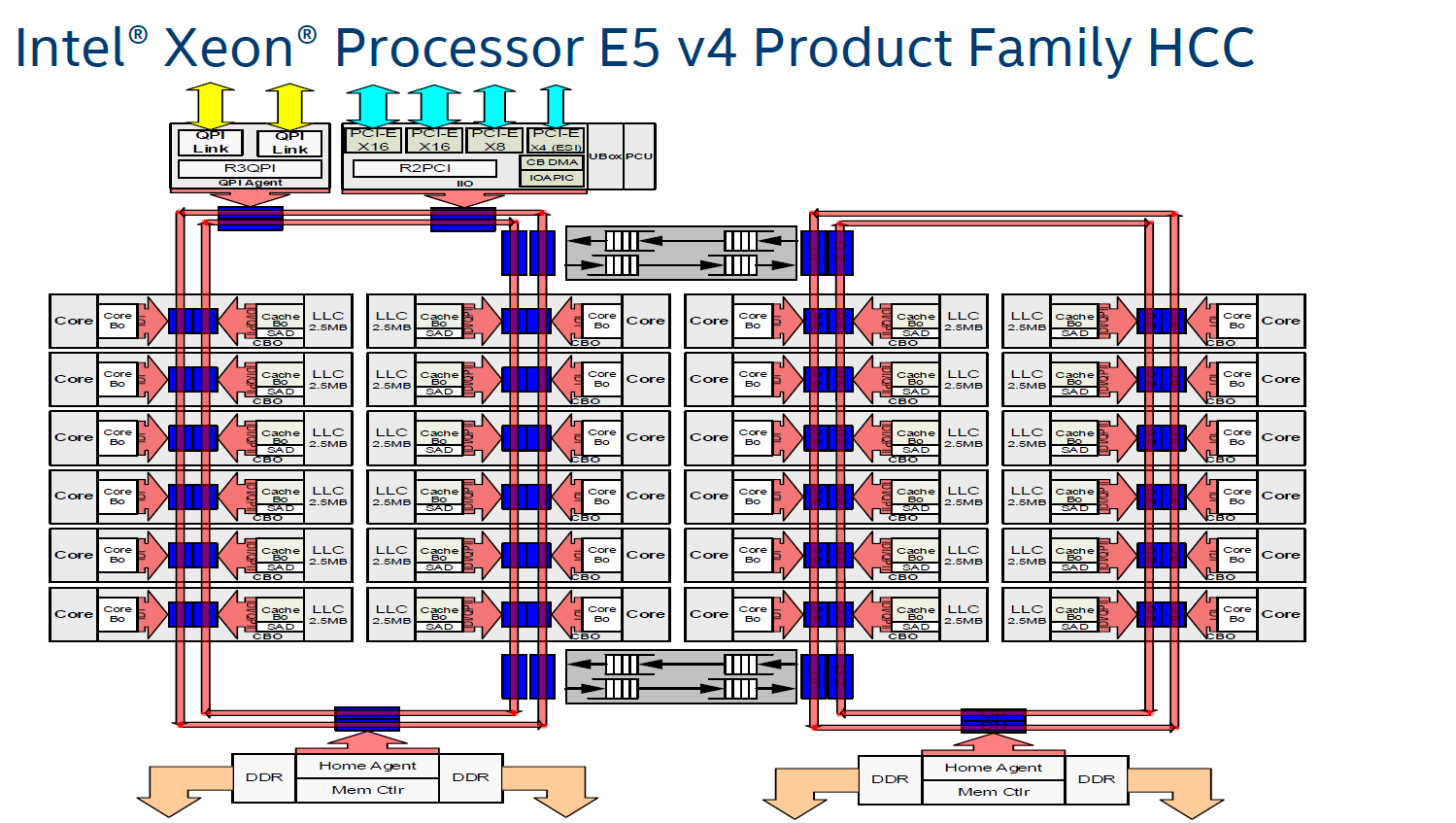
Mesh bus (Xeon Scalable family):#
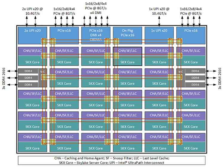
Multi-socket configurations:#
A 4-socket ring configuration:

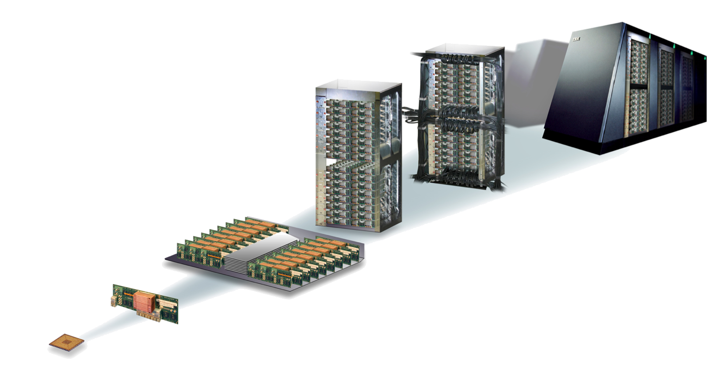
Multiple nodes go into racks or cabinets#

Terminology:#
Core (virtual and physical): has a single program counter (logically sequential processing of instructions)
Memory channel: e.g., DDR4-2400: transfers 64 bits (8 bytes) at a rate of 2400 MHz = 15.36 GB/s
Socket or CPU: contains multiple cores in a single piece* of silicon
Non-Uniform Memory Access (NUMA): different channels may be different distances from a core
Compute node: one or more sockets, plus memory, network card, etc.
2. Memory#
2.1 Cache#
Caches are low-capacity, high-speed memories that are commonly integrated on the CPU die. The need for caches can be easily understood by realizing that data transfer rates to main memory are painfully slow compared to the CPU’s arithmetic performance.
While peak performance soars at several GFlops/sec per core, memory bandwidth, i.e., the rate at which data can be transferred from memory to the CPU, is still stuck at a couple of GBytes/sec, which is entirely insufficient to feed all arithmetic units and keep them busy continuously.
This tells us that Moore’s Law, which for more than thirty years reassured scientists that no matter which technology was implemented to build computer chips, their “complexity” or general “capability” doubled about every 24 months, is not only not valid anymore, but even if it was, it would not be useful in increasing performance on modern complex architectures.
To make matters worse, in order to transfer a single data item (usually one or two Douple Precision (DP) words) from memory, an initial waiting time called latency passes until data can actually flow. Thus, latency is often defined as the time it takes to “transfer a zero-byte message”.
Memory latency is usually of the order of several hundred CPU cycles and is composed of different contributions from memory chips, the chipset and the processor.
Advances in memory performance show up at a much slower rate than the rate of improvement in chip complexity. The term DRAM gap has been coined for the increasing “distance” between CPU and memory in terms of latency and bandwidth.
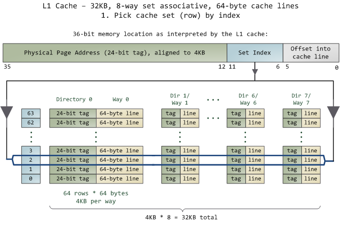
Caches can alleviate the effects of the DRAM gap in many cases. Usually there are at least two levels of cache , called L1 and L2, respectively.
L1 is normally split into two parts, one for instructions (I-cache, L1I) and one for data (L1D).
Outer cache levels are normally unified, storing data as well as instructions.
In general, the “closer” a cache is to the CPU’s registers, i.e., the higher its bandwidth and the lower its latency, the smaller it must be to keep administration overhead low.
How is memory accessed?#
Whenever the CPU issues a read request (”load”) for transferring a data item to a register, first-level cache logic checks whether this item already resides in cache.
If it does, this is called a cache hit and the request can be satisfied immediately, with low latency.
In case of a cache miss, however, data must be fetched from outer cache levels or, in the worst case, from main memory.
If all cache entries are occupied, a hardware-implemented algorithm evicts old items from cache and replaces them with new data.
The sequence of events for a cache miss on a “write” is generally more involved.
Instruction caches are usually of minor importance since scientific codes tend to be largely loop-based; I-cache misses are rare events compared to D-cache misses.
Caches can only have a positive effect on performance if the data access pattern of an application shows some locality of reference. More specifically, data items that have been loaded into a cache are to be used again “soon enough” to not have been evicted in the meantime. This is also called temporal locality.
Unfortunately, supporting temporal locality is not sufficient. Many applications show streaming patterns where large amounts of data are loaded into the CPU, modified, and written back without the potential of reuse “in time”.
In order to reduce the latency penalty for streaming, caches feature a peculiar organization into cache lines.
The advantage of cache lines is that the latency penalty of a cache miss occurs only on the first miss on an item belonging to a line. The line is fetched from memory as a whole; neighboring items can then be loaded from cache with much lower latency, increasing the cache hit ratio.
So if the application shows some spatial locality (as it often appens when discretizing Partial Differential Equations (PDEs)), i.e., if the probability of successive accesses to neighboring items is high, the latency problem can be significantly reduced.
The downside of cache lines is that erratic data access patterns are not supported.
On the contrary, not only does each load incur a miss and subsequent latency penalty, it also leads to the transfer of a whole cache line, polluting the memory bus with data that will probably never be used.
The effective bandwidth available to the application will thus be low.
On the whole, however, the advantages of using cache lines prevail, and very few processor manufacturers have provided means of bypassing the mechanism.
How we define what limits performance:#
When performance is governed by main memory bandwidth and latency — the code is memory-bound.
In order for an application to be truly cache-bound, i.e., decouple from main memory so that performance is not governed by memory bandwidth or latency any more, the cache hit ratio (sometimes denoted by \(\gamma\)) must be large enough so the time it takes to process in-cache data becomes larger than the time for reloading it. If and when this happens depends of course on the details of the operations performed.
How your program accesses memory:#
double a[1000];

void foo() {
    for (int i=0; i<1000; i++)
        a[i] = 1.234 * i;
}
The compiler turns the loop body into instructions, which we can examine using Godbolt.
pxor xmm0, xmm0                  ; zero the xmm0 register
cvtsi2sd xmm0, eax               ; convert the integer i to double
mulsd xmm0, xmm1                 ; multiply by 1.234 (held in xmm1)
movsd QWORD PTR a[0+rax*8], xmm0 ; store to memory address a[i]
Only one instruction here accesses memory, and the performance will be affected greatly by where that memory resides (which level of cache, where in DRAM).
Most architectures today have 64-byte cache lines: all transfers from main memory (DRAM) to and from cache operate in units of 64 bytes.
Let’s compare three code samples#
for (int i=0; i<N; i++)
    a[i] = b[i];
for (int i=0; i<N; i++)
    a[i] = b[(i*8) % N];
for (int i=0; i<N; i++)
    a[i] = b[random() % N];
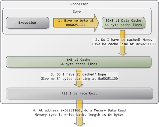
What happens when you request a cache line?#
Operating system effects#
Most systems today use virtual addressing, so every address in your program needs to be translated to a physical address before looking for it (in cache or memory). Fortunately, there is hardware to assist with this: the Translation Lookaside Buffer (TLB).

Further resources:#
List of frequently found acronyms and abbreviations:#
Acronym |
Meaning |
|---|---|
ASCII |
American standard code for information interchange |
ASIC |
Application-specific integrated circuit |
BIOS |
Basic input/output system |
BLAS |
Basic linear algebra subroutines |
CAF |
Co-array Fortran |
ccNUMA |
Cache-coherent nonuniform memory access |
CFD |
Computational fluid dynamics |
CISC |
Complex instruction set computer |
CL |
Cache line |
CPI |
Cycles per instruction |
CPU |
Central processing unit |
CRS |
Compressed row storage |
DDR |
Double data rate |
DMA |
Direct memory access |
DP |
Double precision |
DRAM |
Dynamic random access memory |
ED |
Exact diagonalization |
EPIC |
Explicitly parallel instruction computing |
Flop |
Floating-point operation |
FMA |
Fused multiply-add |
FP |
Floating point |
FPGA |
Field-programmable gate array |
FS |
File system |
FSB |
Frontside bus |
GCC |
GNU compiler collection |
GE |
Gigabit Ethernet |
GigE |
Gigabit Ethernet |
GNU |
GNU (is not UNIX) |
GPU |
Graphics processing unit |
GUI |
Graphical user interface |
HPC |
High performance computing |
HPF |
High performance Fortran |
HT |
HyperTransport |
IB |
InfiniBand |
ILP |
Instruction-level parallelism |
IMB |
Intel MPI benchmarks |
I/O |
Input/output |
IP |
Internet protocol |
JDS |
Jagged diagonals storage |
L1D |
Level 1 data cache |
L1I |
Level 1 instruction cache |
L2 |
Level 2 cache |
L3 |
Level 3 cache |
LD |
Locality domain |
LD |
Load |
LIKWID |
Like I knew what I’m doing |
LRU |
Least recently used |
LUP |
Lattice site update |
MESI |
Modified/Exclusive/Shared/Invalid |
MI |
Memory interface |
MIMD |
Multiple instruction multiple data |
MIPS |
Million instructions per second |
MMM |
Matrix–matrix multiplication |
MPI |
Message passing interface |
MPMD |
Multiple program multiple data |
MPP |
Massively parallel processing |
MVM |
Matrix–vector multiplication |
NORMA |
No remote memory access |
NRU |
Not recently used |
NUMA |
Nonuniform memory access |
OLC |
Outer-level cache |
OS |
Operating system |
PAPI |
Performance application programming interface |
PCI |
Peripheral component interconnect |
PGAS |
Partitioned global address space |
PLPA |
Portable Linux processor affinity |
POSIX |
Portable operating system interface for Unix |
PPP |
Pipeline parallel processing |
PVM |
Parallel virtual machine |
QDR |
Quad data rate |
QPI |
QuickPath interconnect |
RAM |
Random access memory |
RISC |
Reduced instruction set computer |
RFO |
Read for ownership |
SDR |
Single data rate |
SIMD |
Single instruction multiple data |
SISD |
Single instruction single data |
SMP |
Symmetric multiprocessing |
SMT |
Simultaneous multithreading |
SP |
Single precision |
SPMD |
Single program multiple data |
SSE |
Streaming SIMD extensions |
ST |
Store |
STL |
Standard template library |
SYSV |
Unix System V |
TBB |
Threading building blocks |
TCP |
Transmission control protocol |
TLB |
Translation lookaside buffer |
UMA |
Uniform memory access |
UPC |
Unified parallel C |